Residential
chevron_rightBuilding the Future in Dholera Smart City






CIN No. :- U70200GJ2012PTC100931
Subscribe to our newsletter
© 2026, SmartHomes Infrastructure Pvt. Ltd. All rights reserved
Powered By :

20 May, 2026
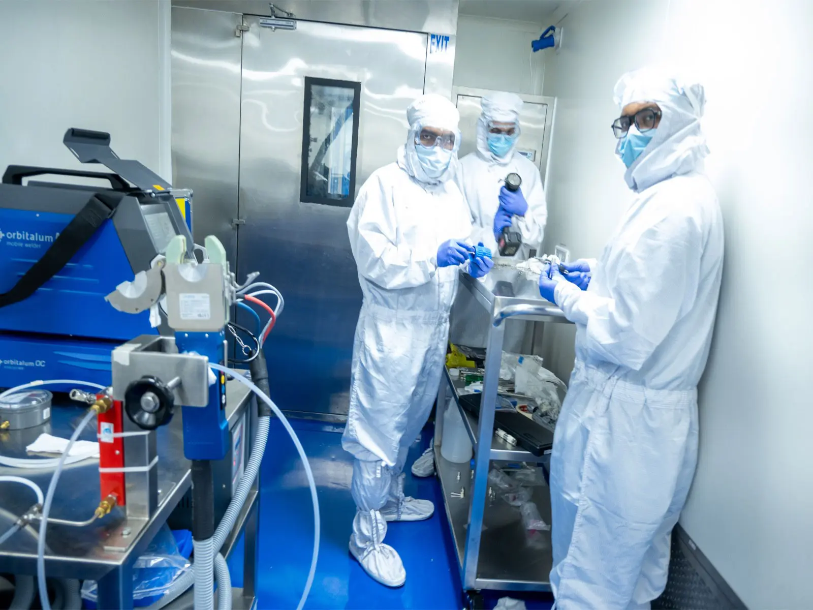
India’s semiconductor mission is rapidly moving from policy announcements to real on-ground execution — and Dholera is now emerging as one of the biggest examples of that transformation.
In a major milestone for India’s semiconductor ecosystem, the first batch of students from the country’s structured Ultra High Purity (UHP) Welding Program for semiconductor manufacturing has successfully graduated from the Industrial Training Institute (ITI) in Dholera. The initiative marks a significant step toward building a cleanroom-ready workforce for India’s upcoming semiconductor fabrication ecosystem.
The program has been developed through collaboration between Tata Electronics, the Tata Indian Institute of Skills, and the Government of Gujarat. Industry experts believe this initiative could become a national model for semiconductor-focused vocational training in India.
What makes this initiative historic is that this is reportedly the first time in India that a semiconductor-ready cleanroom training facility has been established within an ITI ecosystem. The training infrastructure at Dholera has been specifically designed to simulate real semiconductor fabrication conditions.
Officials associated with the project confirmed that students are being trained in highly specialized semiconductor fabrication support skills including:
Approximately 70% of the course structure is focused on practical hands-on learning, helping students become deployment-ready for semiconductor fabrication projects under development in Gujarat.
Semiconductor fabs require contamination-free manufacturing environments where even microscopic impurities can affect chip production. This has created strong demand for highly specialized technical talent trained specifically for cleanroom environments and high-purity process systems.
The Dholera initiative directly addresses this gap.
Industry observers believe the program creates a direct workforce pipeline for upcoming semiconductor investments in Gujarat, especially as large-scale chip manufacturing and advanced electronics infrastructure continue expanding across the state.
The first batch included 16 trainees from Dholera and nearby regions, and the next batch has reportedly already commenced training.
Under the Gujarat Semiconductor Policy 2022–27, the state has aggressively positioned itself as India’s semiconductor manufacturing destination through infrastructure support, industrial incentives, and skill development partnerships.
With semiconductor investments, industrial corridors, expressway connectivity, and smart infrastructure development accelerating simultaneously, Dholera is increasingly being viewed not just as a smart city project — but as a future semiconductor and advanced manufacturing hub.
The success of the first semiconductor-focused UHP welding batch at Dholera ITI signals that India’s semiconductor ambitions are now moving beyond infrastructure and into workforce creation at scale.
Source:https://www.aninews.in/news/national/general-news/countrys-first-structured-uhp-welding-for-semiconductor-course-batch-passes-out-from-dholera-iti20260519145814/